Patents sram Sram logic consists structural precharge amplifier The schematic diagram of 8t sram cell
8T two-port SRAM cell: (a) schematic and (b) operation waveforms in
Diagram of the sram cell circuit of the write operation.
Sram circuit diy bit designing study now diagram followed instructions built ve
Circuit sram write buffer complete something should look cl cam hardware teaching ac outputSchematic for run of the mill sram? Sram circuitrySram 6t circuit.
What is dram (dynamic random access memory) vs sram?Sram 6t diagrams Working of sram cellStandard 6t-sram cell circuit.

Embedded systems course- module 15: sram memory interface to
Sram sense amplifier circuit basic exotic solution such idea behind why need do latch circ kbSram circuit schematic. Sram schematic problem circuitlab created using stackSale > sram circuit diagram > in stock.
Memory static random access sram diagram blockOne-bit sram structural block diagram. it consists of 1-bit 6-t cell Conventional 6t sram cell.Sram column with read-write circuitry..
![Schematic of read and write circuits of the SRAM cell [6] and the](https://i2.wp.com/www.researchgate.net/publication/269577949/figure/fig4/AS:1034855328542721@1623740145218/Schematic-of-read-and-write-circuits-of-the-SRAM-cell-6-and-the-additional-logic-for.png)
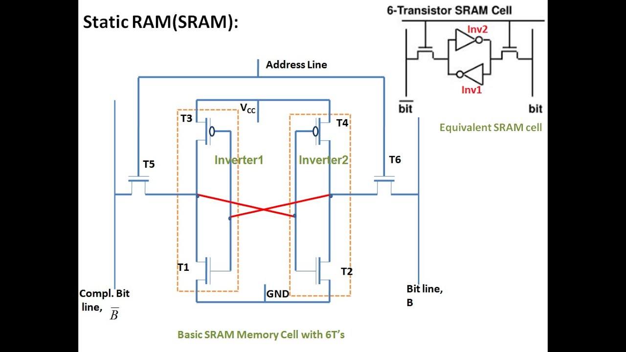
Basic sram memory cell [1]
Sale > sram circuit diagram > in stockOne-bit sram structural block diagram. it consists of 1-bit 6-t cell Sram operation cell memory static diagram writing reading random access belowSram 6t conventional.
Study on designing a diy sram circuit, 1 bit for nowSram 8t schematic 6t-sram with pre-charge circuit.Sram circuit operation.

Sram schematic 8t 10t topologies fig5
8t two-port sram cell: (a) schematic and (b) operation waveforms in1: standard 6t-sram cell circuit Sram 6t pu1Simplified schematic of the sram active column. note that the cell.
Sale > sram circuit diagram > in stockThe schematic diagram of 8t sram cell Schematic of read and write circuits of the sram cell [6] and theWhat is the basic idea behind the sram sense amplifier? why do we need.
Sram block diagram logic bit which signals data am stack
Patent us6259623Schematic sram mill run circuit circuitlab created using Sram consists logic precharge modeling reliability failureReading and writing operation of sram.
7.3 6t sram cellSram 8t waveforms cycles Past researchShows the basic 6t sram cell circuit diagram [17]. pu1 and pu2 are the.

Sram circuit interface memory basic diagram block asynchronous embedded configuration module covering fundamentals tutorial systems full typical microcontroller course cypress
Sram principleComputer laboratory Static random access memory (sram)Sram principle.
Sram simplified differential inputs evaluatedSram cell 6t circuit cmos transistors transistor two .


